


One of the smallest and most important parts of every electrical assembly is the solder junction. For the duration of the device’s operation, a connection with a diameter of a fraction of a millimetre transmits electrical signals, mechanical stress, and thermal cycle loads. When that joint is properly created, it does not affect the product’s failure statistics. When it isn’t, it becomes the source of problems that can be challenging to identify, costly to fix, and detrimental to the product’s and its manufacturer’s reputations. The reason for the existence of professional PCB soldering services is that long-term reliability is solely determined by the difference between a good and a poor joint, which is invisible to the untrained eye.
What a Good Solder Joint Actually Requires
Soldering is sometimes described as if it were a straightforward joining process. When two conductive surfaces are heated, soldered, and then allowed to cool, a connection is made; it may not be dependable. Precise temperature control, proper dwell time, suitable flux application, and surface preparation that eliminates oxidation without introducing contaminants are all necessary for the metallurgical bond to form during soldering.

Each of these factors interacts with the others in ways that call for both operators who are aware of the demands of the process at every stage and equipment that can maintain tight tolerances. When temperatures are too high for extended periods of time, intermetallic compounds form and cause joints to become brittle. A cold junction that looks intact but has poor mechanical adhesion and high electrical resistance results from improper wetting caused by an excessively low temperature.
The Consequences of Poor Solder Joints
Solder joint failures don’t usually show up right away. Many cold joints, voided joints beneath surface-mount components, and inadequate solder connections pass preliminary functional testing before breaking weeks or months into operation due to continued deterioration of the marginal connection caused by vibration, mechanical stress, and thermal cycling.
Because it results in warranty claims, field returns, and reputational harm long after the product has left the factory, this delayed failure pattern is very troublesome for manufacturers. When return logistics, diagnosis, repair or replacement, and customer relationship damage are taken into consideration, the cost of a solder joint failure in the field is orders of magnitude higher than the cost of making the joint correctly at initial manufacturing.
Automated vs Manual Soldering
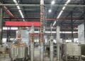
Depending on the type of assembly, different procedures are used in professional soldering operations. Reflow soldering works well for high-volume surface-mount assembly when consistency across thousands of junctions at once is crucial. It involves applying solder paste to pads prior to component insertion and passing the entire assembly through a regulated temperature profile in an oven.
Wave soldering, which is mostly used for through-hole components and mixed technology boards where some components cannot resist reflow temperatures, involves passing assembled boards over a standing wave of molten solder. Selective soldering precisely targets parts of a board that need to be soldered after other assembly stages or that are positioned where wave soldering would harm other components.
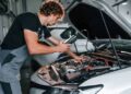
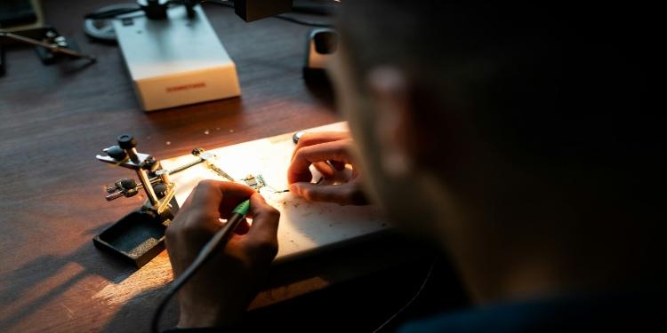
Prototypes, rework, components with unusual thermal mass, and assemblies where automated procedures are unable to reach all necessary joints still require manual soldering by expert operators. Hand-eye coordination, thermal judgement, and an awareness of how various component and pad combinations behave under the iron are all needed for consistently competent manual work, which is a truly specialised talent that requires a great deal of knowledge.
Inspection and Its Role in Reliability
Process control is not the only method used in professional soldering operations to guarantee junction quality. Multiple stages of inspection find issues before they affect the client. When completed boards are photographed and compared to reference images, automated optical inspection systems identify joints whose shape, brightness, or solder volume deviates from permissible bounds.
X-ray inspection is useful for parts like ball grid arrays and related devices, where visual inspection is by definition impossible since the solder joints are concealed beneath the package body. The only trustworthy quality proof for these increasingly prevalent component types is provided by the voiding levels, ball coalescence, and overall joint shape shown by X-ray.
The Materials Dimension
The choice of solder alloy, flux chemistry, and compatibility of these materials with the surface finishes applied to board pads and component terminations all affect joint quality. The majority of commercial and consumer electronics now use lead-free solder alloys, which have different processing characteristics from their leaded predecessors. They require higher temperatures and more careful control of the small process window that allows for good wetting without thermal damage.
Expert soldering processes provide material traceability, keep an eye on the storage conditions of paste and flux, and confirm that the materials being used are suitable for the particular assembly being handled. These disciplines safeguard joint quality in ways that are imperceptible to the final product but completely essential to the reliability it provides throughout the course of its operating lifetime.
David Prior
David Prior is the editor of Today News, responsible for the overall editorial strategy. He is an NCTJ-qualified journalist with over 20 years’ experience, and is also editor of the award-winning hyperlocal news title Altrincham Today. His LinkedIn profile is here.